
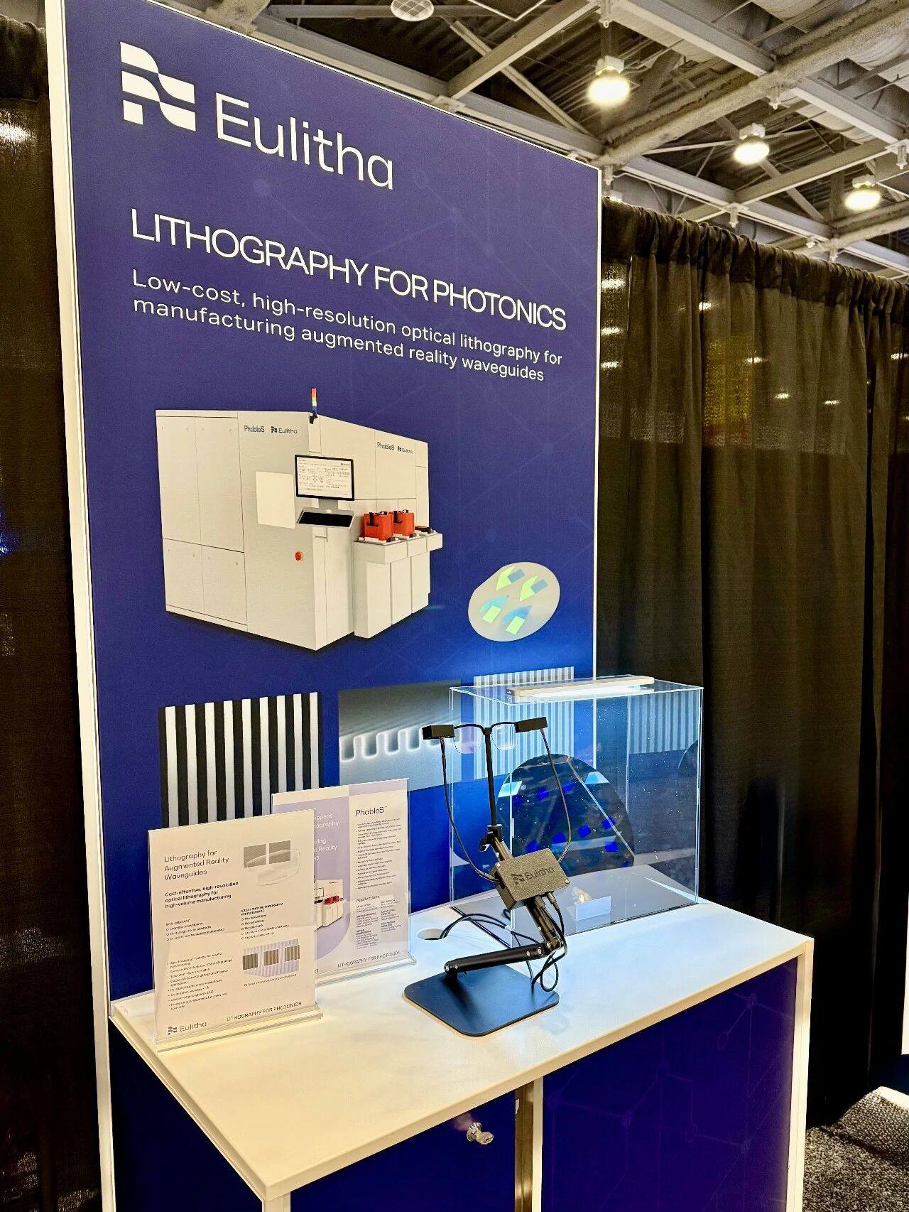
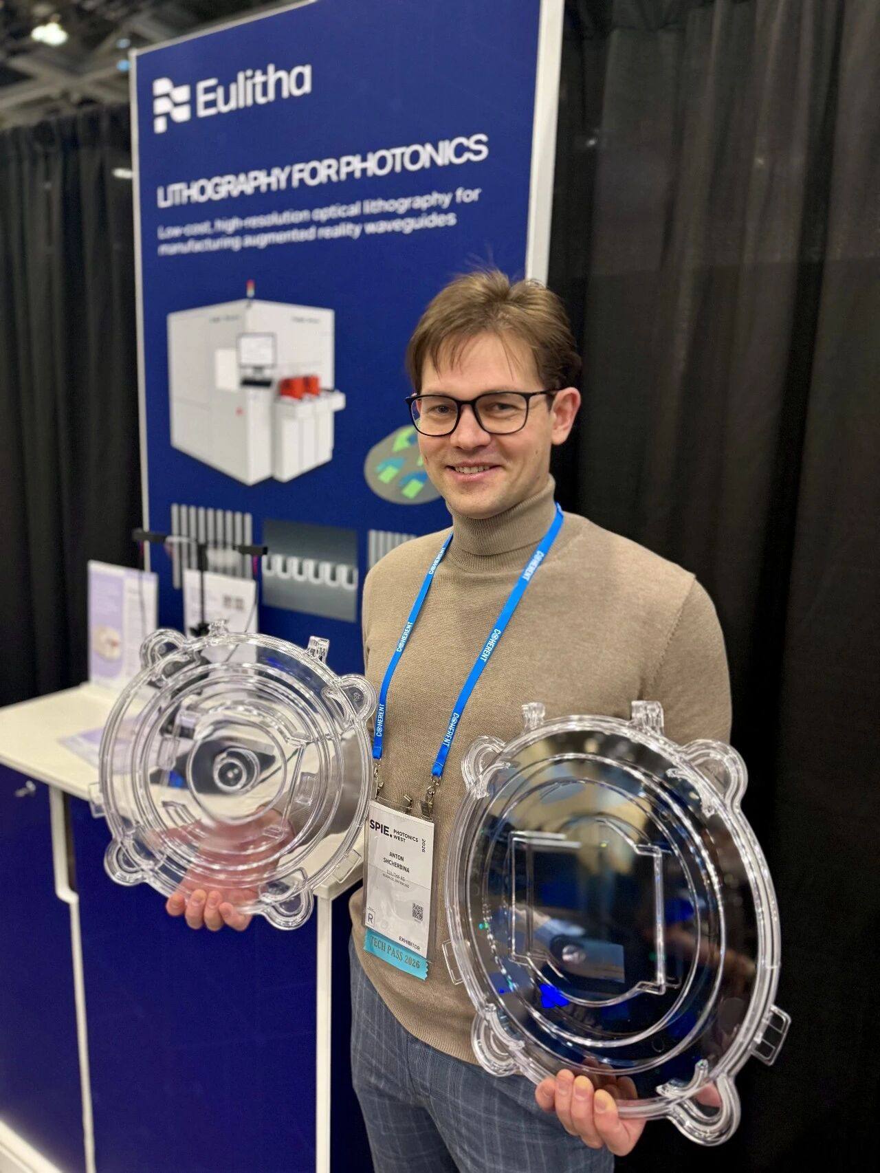
在 SPIE 2026 期间,先进光刻技术领导者 Eulitha 与 AR 衍射光波导制造商广纳四维(SEEV)联合展示关键工艺成果。基于 Eulitha 位移泰伯光刻(DTL)技术制备的广纳四维碳化硅刻蚀全彩样品亮相展会现场,标志着双方合作已将高性能 AR 光学器件的量产能力推至新高度。
During SPIE 2026, advanced lithography leader Eulitha and AR diffractive waveguide manufacturer SEEV jointly presented key process achievements. Waveguide samples showcased at the event included SEEV's silicon carbide (SiC) etched fullcolor waveguides fabricated based on Eulitha's Displacement Talbot Lithography (DTL) technology. This demonstration signifies that the collaboration between the two parties has elevated mass-production capabilities for high-performance AR optical components to a new level.
精密光刻与半导体工艺的深度结合
In-Depth Integration of Precision Lithography and Semiconductor Processes
衍射光波导的制造本质是半导体微纳工艺在光学上的精密应⽤。Eulitha 的 DTL 技术可在 4 至12 英寸衬底上实现高均匀性图案化,分辨率达 65nm,并具备大曝光场、无拼接、曲⾯衬底兼容等优势,显著提升了 AR 光波导的制造效率,为规模化⽣产奠定了设备基⽯。
The manufacturing of diffractive waveguides is inherently a precise application of semiconductor micro/nano-fabrication processes in optics. Eulitha's DTL technology offers high-uniformity patterning on substrates ranging from 4 to 12 inches, achieving resolutions down to 65 nm. The technology offers significant advantages, including a large exposure field, stitch-free operation, and compatibility with curved substrates, substantially improving manufacturing efficiency for photonic devices such as AR waveguides, laying essential equipment groundwork for large-scale production.
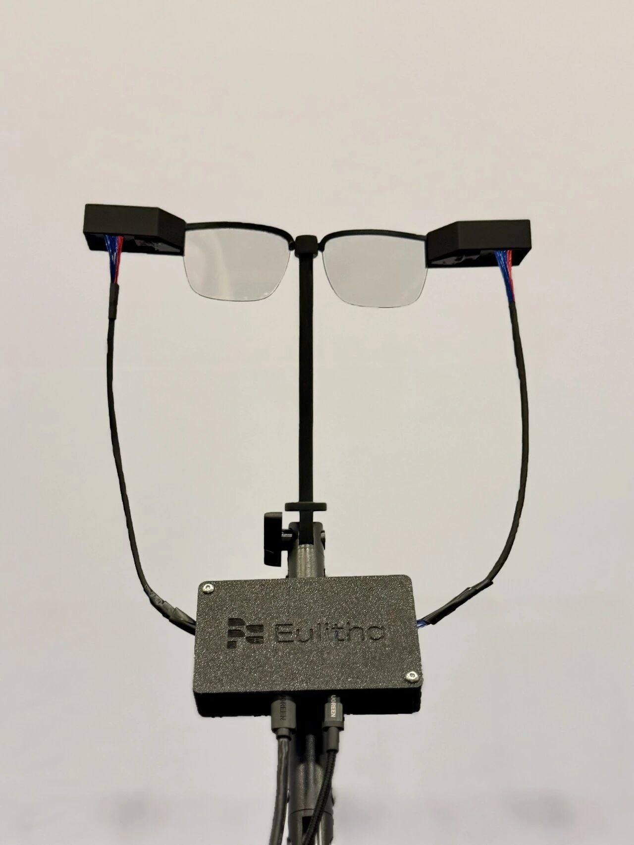
广纳四维的核心战略,是将成熟的半导体制造工艺体系全面引入AR 光学领域,并采⽤ IDM 垂直整合制造模式,实现设计、工艺与制造的全链条⾃主。基于此,广纳四维成功开发了专有的刻蚀与掩模⽅案,能驾驭如碳化硅 SiC 等硬质材料,实现复杂的全彩光栅结构,显著提升器件性能与良率。
SEEV's core strategy involves fully introducing mature semiconductor manufacturing processes into the AR optics field and adopting an IDM (Integrated Device Manufacturing) model to achieve full-chain autonomy encompassing design, process, and manufacturing. Based on this approach, SEEV has successfully developed proprietary etching and mask schemes capable of processing hard materials like silicon carbide (SiC) to create complex full color grating structures, significantly enhancing device performance and production yield.
生态协同,相互成就
Synergistic Ecosystem, Mutual Success
此次联合成果,体现了设备与工艺深度协同的产业价值。广纳四维基于半导体工艺与IDM 模式所实现的突破,是 Eulitha DTL 技术在尖端光学制造中卓越能力的有力证明;而Eulitha 稳定、高性能的光刻平台,则是广纳四维实现技术蓝图与可靠量产的基石支撑。此次展示,标志着双方已超越传统的供应链合作,成为推动 AR 光学制造边界拓展的“关键生态伙伴”。
This joint achievement highlights the industrial value of deep collaboration between equipment and processes. The breakthroughs realized by SEEV, based on semiconductor processes and the IDM model, strongly demonstrate the exceptional capabilities of Eulitha's DTL technology in cutting-edge optical manufacturing. Conversely, Eulitha's stable, high-performance lithography platform provides the foundational support for SEEV to realize its technological roadmap and achieve reliable mass production. This showcase indicates that the partnership has transcended the traditional supplier-client model, evolving into a "key ecosystem partnership" driving the expansion of AR optical manufacturing boundaries.
广纳四维与 Eulitha 所展现的深度协同模式,不仅为 AR 眼镜迈向更优显示与可靠量产提供了核心保障,也为光子学器件与半导体先进制造的融合树立了典范。双方将继续深化合作,共同推动 AR 光学乃至更为广泛的光子集成领域制造技术的进步。
The deep collaboration model demonstrated by SEEV and Eulitha not only provides core assurance for AR glasses to achieve superior display performance and reliable mass production but also sets an example for the integration of photonic devices and advanced semiconductor manufacturing. The two companies will continue to deepen their cooperation to jointly advance manufacturing technologies in AR optics and broader photonic integration fields.
企业简介
Company Profiles
广纳四维(SEEV)
公司专注 AR 衍射光波导微纳光学器件的研发与批量化生产,并率先将成熟的先进半导体制造工艺引⼊ AR 光学领域,掌握了从光学设计、材料、纳⽶加工到器件封测的全链条核心技术与生产能力。通过创新的晶圆级碳化硅刻蚀工艺,广纳四维不仅提升了光学器件性能,也为智能穿戴设备的发展提供了新的可能性。
The company focuses on the R&D and batch production of AR diffractive waveguide micro-nano optical devices. It is a pioneer in introducing mature advanced semiconductor manufacturing processes into the AR optics field, mastering core technologies and production capabilities across the entire chain from optical design, materials, and nano-processing to device packaging and testing. Through its innovative wafer-level silicon carbide (SiC) etching process, SEEV not only enhances the performance of optical components but also creates new possibilities for the development of smart wearable devices.
优利赛尔(EULITHA)
Eulitha specializes in high resolution, high-throughput non-contact deep ultraviolet (DUV) lithography systems. The Phable series (PhableR/X/S) caters to diverse needs from R&D to mass production, providing scalable solutions for both research and industrial applications. To strengthen local support, Eulitha established a wholly owned subsidiary in Beijing in 2023, Eulitha Beijing Co., Ltd and built a Demo Lab. This facility offers customized process support and rapid response services to customers in the Asia-Pacific region, advancing industrial innovation in semiconductors and photonics.
来源:广纳四维